2022 Featured Research

Dr. William Vandenberghe
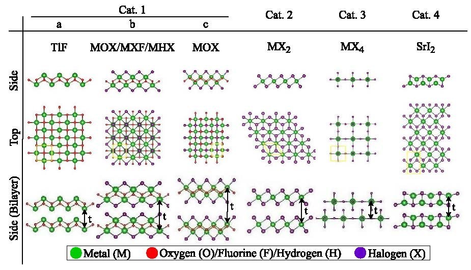
Two-dimensional (2D) materials promise great advantages for future nanoelectronic devices. In a paper published in Nature Communications entitled “Identification of two-dimensional layered dielectrics from first principles” Dr. William Vandenberghe, associate professor of materials science and engineering, and his research team describe how they scanned databases containing 2D materials and identified 32 candidate materials. The candidate materials can be classified in five different categories and the atomic structure is illustrated in our Figure. Investigating each of the 32 materials in more detail, the group found that oxyhalide materials like lanthanum oxychloride are a very promising category of 2D dielectrics that need more experimental attention. Their findings were recognized funding agencies and recently Dr. Bing Lv an associate professor of physics at UT Dallas, and Vandenberghe received an award from the Office of Naval Research for an experimental investigation of oxyhalides.
Dr. Massimo Fischetti
The miniaturization of transistors has driven the tremendous progress of microelectronics that shapes our lives. So far, silicon has been the semiconductor of choice. However, as the dimensions of transistors reaches a few billionth of a meter (nanometers), silicon may show some limits. Therefore, since graphene was synthesized in 2004, researchers have looked for atomically thin materials that may hopefully replace silicon and allow scientists to continue to miniaturize transistors even more.
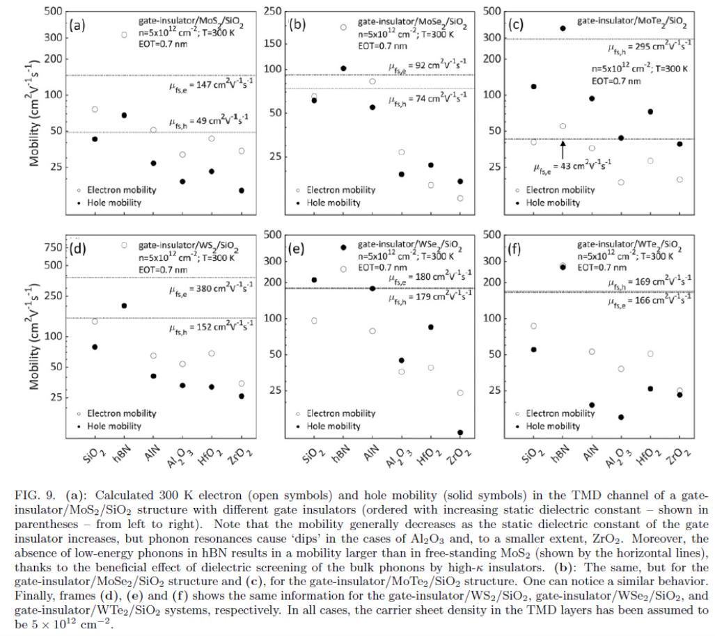
Layers as thin as a single atom, also called monolayers, of transition metal dichalcogenides tungsten diselenide (TMDs), such as molybdenum disulfide or tungsten diselenide, have been studied experimentally and theoretically. Theoretical studies of how fast electrons move in these monolayers have focused almost exclusively to free-standing layers. However, in transistors, these layers are supported by an insulating substrate and are covered by a gate insulator. Dr. Massimo Fischetti, holder of the Texas Instruments Distinguished Chair in Nanoelectronics and professor of materials science and engineering at UT Dallas, and authors of a recent article published by Cornell University have studied theoretically the effects of these insulators (or ‘dielectrics’) on the charge transport properties of TMD monolayers. They have used well-known methods from the beginning to calculate the low-field carrier mobility in free-standing layers and have used the dielectric continuum approximation to extend their study to layers in double-gate structures, including the effects of dielectric screening of the electron-phonon interaction (that is, the collisions of electrons with the vibrations of the atoms constituting the layer) caused by the bottom oxide and the gate insulator. They have also studied scattering with a particular type of oscillations that result from the interaction of plasma oscillations of the electrons in the monolayer and optical phonons on the insulators, a process called remote phonon scattering. They found that the presence of insulators with a high dielectric constant may significantly improve the carrier mobility. However, remote-phonon scattering negates this gain and degrades the mobility significantly below its free-standing value.
The authors have also identified the most promising combination of supporting substrate, TMD monolayer and top-gate insulator of silicon dioxide, tungsten diselenide and hexagonal boron nitride, whereas a realistic combination of materials including silicon dioxide, tungsten diselenide and hafnium oxide, while required by transistor-scaling, is predicted to exhibit poor charge-transport properties.
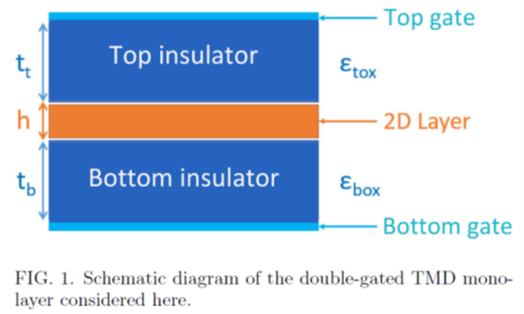
field-effect transistor with a channel based on a transition-metal
dichalcogenide (TMD) monolayer. The bottom-gate substrate is assumed to
be silicon dioxide and the top-gate insulator can be any of the
insulators with a high dielectric constant that are considered by the
nanoelectronic industry. The thickness of the top is depicted
above, while h denotes the thickness of the TMD monolayer, including the
van der Waals gaps.

Dr. Julia Hsu
Halide perovskite, such as methylammonium lead iodide (MAPbI3), has drawn much attention in the photovoltaic industry in the past decade, due to its low-cost, solution processability, and excellent defect tolerance. However, all the highest efficiency perovskite solar cells (PSCs) are laboratory-based and are made using hot plates to convert the precursor to a photo-active perovskite phase at 100 – 170 degrees Celsius for 10−60 min. The inherently long process time and high energy usage of thermal annealing tools are obstacles to scaling up PSC production.
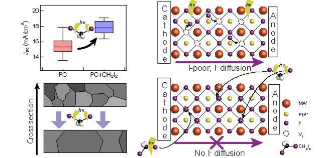
Dr. Julia Hsu, holder of the Texas Instruments Distinguished Chair in Nanoelectronics and professor of materials science and engineering, and her research group are focusing on replacing the long thermal annealing process in the PSC fabrication with a high-throughput process called photonic curing. Photonic curing uses a xenon lamp to deliver energy to the sample in short pulses from 20 microseconds to 100 microseconds pulses. The precursor films absorb the radiant energy from the light pulses and convert them to the perovskite phase. The group has previously demonstrated that this technique can complete the conversion to perovskite in a few milliseconds. Most recently, they achieved a champion photonically cured device with a power conversion efficiency of 15.02% with the addition of diiodomethane to perovskite in p-i-n devices, which is comparable to the thermally annealed device with efficiency of 15.82%. Diiodomethane is a chemical that can be easily dissociated under the light. They found that diiodomethane addition only improves photonically cured PSCs, not thermally annealed PSCs. They confirmed that photonically cured MAPbI3 films have a lower iodine concentration. The addition of diiodomethane in photonically cured MAPbI3 films recovers the lead/iodine stoichiometry. More than that, the bulk resistance of photonically cured MAPbI3 films is reduced, and the ionic diffusion is slowed after adding diiodomethane. Their finding adds an understanding of additive mechanisms for perovskite processing using light, which is different from thermal processes. The results indicate that photonic curing is a promising annealing technique for high-throughput PSC manufacturing.
This work, “Elucidating Diiodomethane-Induced Improvement in Photonically Cured MAPbI3 Solar Cells,” has been published recently in ACS Applied Energy Materials. Contributors include UT Dallas MSE doctoral students and research assistants Weijie Xu and Robert Piper, UT Dallas physics formal research assistant and professor Dr. Yangzi Zheng and Dr. Anton V. Malko.
Dr. Manuel Quevedo
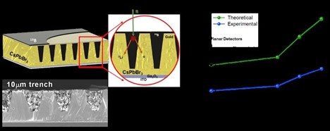
Dr. Manuel Quevedo, professor and head of the Department of Materials Science and Engineering, has demonstrated that a combination of novel techniques such as a solvent-free thin-film deposition, perovskite patterning and a 10B backfill technique enables the high neutron detection efficiency in a perovskite-based microstructured thermal neutron detector. The fabricated and microstructured cesium lead bromide thermal neutron detectors show an efficiency of 4.3%. This represents greater than1.2 times efficiency improvement over planar silicon at 3.5% and greater than two times efficiency improvement over planar CsPbBr3 detector at 2.1%, respectively. More importantly, gamma-ray discrimination of 107 is measured in CsPbBr3-based microstructured neutron detectors.
Dr. Orlando Auciello
Dr. Orlando Auciello, holder of the Distinguished Chair in Engineering and professor of materials science and engineering and bioengineering, studies medical coatings for a variety of applications. His latest book: Ultrananocrystalline Diamond Coatings for New Generation High-Tech and Medical Devices was published in July 2022 by the Materials Research Society through Cambridge Press.