2023 Spring Featured Research
Dr. Orlando Auciello
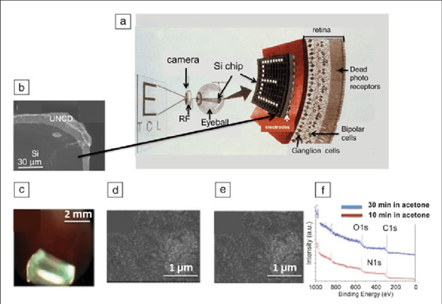
Science and Technology of Transformational Multifunctional Ultrananocrystalline Diamond (UNCDTM) Coating for Industrial/High-Tech/Biomedical Applications
This article describes the science and technology of a transformational coating, named ultrananocrystalline diamond (UNCDTM), and integration into new generations of industrial, high tech medical devices. UNCD films are synthesized by novel processes, using patented argon/methane gas chemistry, generating unique diatomic carbon dimers and contributing benzene, methylene or a methyl radical species, inducing nucleation and growth of UNCD films with the smallest grain size today at 3-5 nanometers.
The combination has unique properties, enabling technological applications including:
- UNCD-coated mechanical pump seals and bearings.
- UNCD films on atomic force microscopy tips, without mechanical degradation as silicon / metal tips.
- UNCD dielectric layer in radio-frequency microelectromechanical system switches, eliminating failure of prior silicon dioxide / silicon nitride dielectric layers.
- Best biocompatible UNCD coating made of carbon atoms, enabling superior medical devices/prostheses.
- UNCD-coated silicon microchip (artificial retina) implantable on eye’s retina, to return partial vision to people blinded by genetically induced degeneration of photoreceptors.
- UNCD-coated dental implants, currently in clinical trials, eliminating failure via corrosion.
- Nitrogen-doped N-UNCD-coated commercial nanograined copper anode, enabling new generation of lithium ion batteries with superior energy capacity.


Dr. Julia Hsu and Dr. William Vandenberghe’ s Groups:
Understanding Morphology Effects on Fill Factor Losses in Dilute-Donor Organic Solar Cells
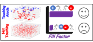
In this article published by Nano Energy, organic solar cells (OSCs) have been the subject of intensive investigations over the last decades because of their solution processability, energy level tunability and materials sustainability. An OSC is fabricated by combining two organic materials: one acting as an electron donor and the other acting as the electron acceptor. In OSCs, light generates an exciton in the material and the exciton is dissociated at the donor-acceptor interface into an electron, traveling along acceptors to the cathode contact, and a hole, moving along donors to the anode contact. Most OSCs have active layers with a bulk heterojunction (BHJ) morphology, consisting of about half donor and half acceptor materials. In BHJ OSCs, donor and acceptor materials form interpenetrating percolative pathways, representing a compromise between fast charge collection and efficient exciton dissociation.
Surprisingly, OSCs fabricated using low donor concentrations also exhibit decent photoresponse. These small donor concentration OSCs are the subject of our present study, and we will refer to them as dilute-donor solar cells (DDSCs). One potential DDSC advantage is to produce open-circuit voltages (Voc) exceeding their BHJ counterpart with comparable short circuit current density (Jsc). While DDSC understanding is emerging, the high Voc and Jsc have unfortunately been accompanied by low fill factors (FFs), lower than in BHJ solar cells. If DDSC FF can be improved, DDSC will be a very attractive solar cell technology.
Experimental results of organic solar cells with low donor concentrations using small molecule donors have displayed significantly lower fill factors (FFs) compared to dilute-donor solar cells (DDSCs) with polymer donors. We perform experiments and kinetic Monte Carlo simulations, to understand the observed FF discrepancy and how FF can be improved. Our results reveal that small molecule DDSCs collect holes from the region of the active layer near the anode whereas polymer DDSCs collect holes from a deeper volume inside the active layer. This enlarged collection region is facilitated by the morphology of polymer chains extending from the anode into the active layer. The chains permit holes to hop along the donor sites to the anode with no barrier. Small molecule DDSCs, in contrast, require a large electric field to transfer holes from isolated donor sites back to the acceptor matrix to reach the anode. Collections in small molecule DDSCs are thus constrained to photogenerated holes on donors near the anode. We propose strategies to increase DDSC FF to levels comparable to bulk-heterojunction organic solar cells by decreasing the donor-acceptor highest occupied molecular orbital energy offset, or by engineering the active layer morphology so that a higher density of donors are in proximity/contact with the anode.

Dr. Kyeongjae Cho
Spin-defect Qubits in Two-dimensional Transition Metal Dichalcogenides Operating at Telecom Wavelengths
In this paper published by Nature, we have discovered a new class of quantum bit (qubit) candidates for quantum information processing. Two-dimensional (2D) semiconductor host crystals can enable the position control of defect placement which can provide the information processing qubit unit. We expect that the 2D defect qubit can overcome the known limitations of the bulk crystalline defect qubits such as diamond NV-center defects. Future research includes experimental confirmation of the discovered 2D defect qubits

Dr. Manuel Quevedo’ s Group:
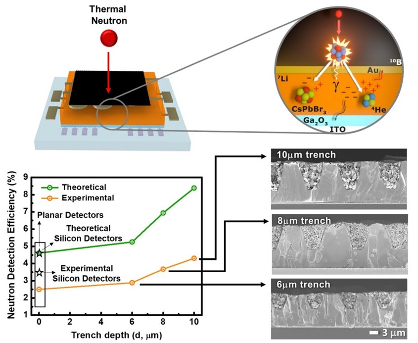
Inorganic Halide Perovskite Thin Films for Neutron Detection
The need for high-efficiency radiation detectors with wide-area coverage is essential in applications such as nuclear medicine, industrial imagining, environmental radioactivity monitoring, spacecraft applications and homeland security, among others. For these applications, the detector material should interact strongly with high-energy particles or photons, must be able to operate at high electric fields with negligible leakage current, must possess high resistivity and must be scalable.
Cesium lead bromide chloride (CsPbBr3-xClx) possesses excellent electric, electronic and spectroscopic properties while showing endurance to humidity and good stability under extreme operating conditions. These properties make it an ideal material for high-energy radiation detectors. The use of CsPbBr3-xClx for heavily charged particle sensing is normally limited to single crystals due to the lack of deposition techniques for thick CsPbBr3-xClx films, which is necessary for efficient radiation and neutron sensing.
This chapter published in Advanced Materials for Radiation Detection shows methods that allow the deposition of perovskite thin films with controlled thickness. The close space sublimation (CSS) process allows for the deposition of stoichiometric and high-quality CsPbBr3-xClx films with reduced defects and large grains with high deposition rates. Alpha and neutron particle sensing using a p-n diode is discussed. This chapter demonstrates the potential of inorganic perovskite films for alpha and neutron detectors in planar and micro-structured perovskite thin films.