
EQUIPMENT AND FACILITIES
Providing students with the necessary equipment to expand on ideas and research is vital in promoting modern innovation. The equipment and facilities described below are housed in the $85 million Natural Science and Engineering Laboratory (NSERL) building. These capabilities will provide graduate students with tools uniquely suited to engage in research areas of modern materials science and engineering. Students are encouraged to learn more about MSE facilities and equipment such as their capabilities and availability.
MSE FACILITIES
ALD Capability – Thin Film Deposition and Characterization
This laboratory has the ability to control and characterize all interfacial regions associated with the high-k dielectric/III-V gate stack. A unique multi-module cluster system is utilized for the fabrication and characterization of dielectric (and contact electrode) films on the III-V substrates.
Learn more on Dr. Jiyoung Kim’s research group page
Computational Materials Science Facilities
Materials modeling software tools and hardware facilities are available for nanoscale materials research. Atomistic modeling software tools are used for structure and dynamic analysis of diverse material systems at nanoscales, and the examples include nanoelectronic materials and nanomaterials for renewable energy applications. Computer programs based on density functional theory (DFT) software tools (VASP, ABINIT, PWSCF, and SIESTA) and empirical-pseudopotential (developed in-house) are used for quantum mechanical analysis of materials. In-house semiclassical (based on the Monte Carlo method) and quantum transport modeling software tool (based on the non-equilibrium Green’s function (NEGF) and the Master equation methods) are used for I-V calculation of nanoelectronic devices .
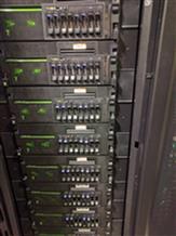
These software tools are available on several computer platforms: 1. A dedicated high-performance cluster consisting of 12 IBM-755 nodes containing 32 IBM Power-7 cores and 256 GB RAM each making for a total of 384 cores and 3 TB RAM; 2. A computational research computing cluster, called Ganymede, that is being developed at UT Dallas. The cluster was started with: 20 Dell R730 computers with dual 20 core CPUS, 256GB RAM four nVidia K1 GPU’s, a high performance parallel storage system running gpfs from DDN, a 100 Gbps capable infiniband interconnect and two 32 port Cisco Nexus 9000 series 10 Gbps Ethernet switches. 3. 11 Linux and AIX workstations which are used to run small workloads and to connect to the several high-performance resources at our disposal. These software and hardware tools are also used for class projects in MSEN 5377.
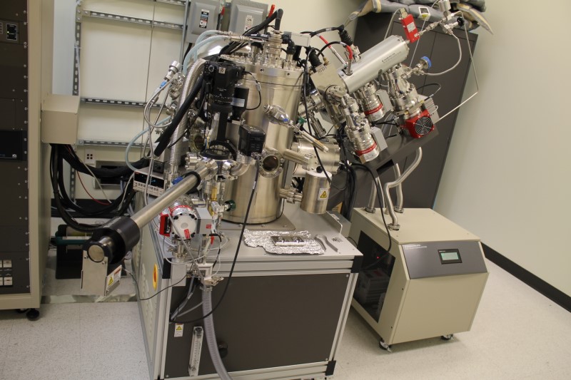
Molecular Beam Epitaxy
A unique multi-chamber MBE has been established with each of the VG-Semicon growth chambers linked together with a UHV transfer tube system operating at a base pressure of about 10-11 mbar. II-VI growth is performed in a V80H growth chamber equipped with two vertical e-beam evaporators, enabling the growth of high melting temperature metals such as Hf, Mo, W, and Fe, in addition to effusion cell evaporation of Se, Te, Zn, Bi, and Be. The two e-beam evaporators allow for TMD and topological insulator heterostructure growth as well as mixed transition metal TMDs and magnetic doping, providing significant flexibility in material and device design. The chamber is also equipped with ZnCl2 and nitrogen plasma sources for doping and surface functionalization. The III-V chamber is also a V80H with recently upgraded hardware and software to provide state-of-the-art growth capabilities including In, Ga, As, B, Al, and N compounds as well as in-situ H-cleaning and Be and Si doping. The Group IV chamber, a V90S, is used to grow Si, Ge, and Sn epitaxial films,SiSnGe compounds, and strained heterostructures. The vertical growth chamber in this system incorporates electron-beam evaporators and effusion cells for Sb and B doping. Preparation chambers with high temperature heating stages are available for each material system. Each growth chamber is equipped with in-situ RHEED allowing us to assess the growth quality in real-time.
Learn more on Dr. Chris Hinkle’s research group page
Multiscale Simulation Lab
This lab focuses on three research themes including Lithium-ion battery, Catalyst and 2D Materials using Density Functional Theory (DFT) Simulation.
Learn more on Dr. Kyeongjae Cho’s research group page
Surface Optical Spectroscopy
The optical spectroscopy laboratory, formally known as the Laboratory for Surface and Nanostructure Modification (LSNM), integrates a number of optical techniques (infrared, Raman, UV-vis spectroscopy and spectroscopic ellipsometry) with homemade chambers and reactors for in-situ studies of surface modification, thin film growth and nano-materials characterization. It includes four Ultra High Vacuum (UHV) chambers and five Atomic Layer Deposition reactors, each one interfaced to a separate FTIR spectrometer. LSNM is used (and in some cases), to develop optical spectroscopic and imaging techniques to explore elementary processes at surfaces and interfaces of technologically important electronic, photonic, organic and more recently biological heterostructures.
Learn more on Dr. Yves Chabal’s research group page
Surface Science System
The system enables detailed studies of surface reactions and structure at the atomic scale.
Learn more on Dr. Robert Wallace’s research group page
UHV Deposition and Characterization Cluster System
The system is capable of thin film deposition using PVD methods including electron beam evaporation, molecular beam deposition, sputter deposition, thermal evaporation, and atomic layer deposition methods.
Learn more on Dr. Robert Wallace’s research group page
Wafer Bonding Laboratory
The wafer bonding laboratory, formally known as the Nano & Beyond Lab, houses an UHV wafer bonding unit, especially designed to use surface characterization and thin-film deposition techniques to measure and control substrate and interface chemistry within limits necessary to make heterojunction devices, is available to produce integrated heterostructures with well controlled chemistry that are tractable for quantitative nanostructural and properties measurements. This unit is capable of synthesizing interfaces by direct wafer bonding and/or in-situ thin film deposition method, and offers greater flexibility for producing advanced integrated artificial structures. It consists of five interconnected ultra high vacuum (UHV) chambers for in-situ surface preparation and analysis, addition of interface interlayers by e-beam or UHV sputter deposition, a bonding chamber, and a sample entry and preparation chamber. The base pressure is 2×10⁻¹⁰ Torr. Orientation of the bonded pairs can be controlled to ~ 0.1 degree prior to bonding. Ex-situ surface preparations using etching and low energy reactive plasma cleaning is done in a cleanroom to protect substrates prior to insertion in the bonding instrument. An atomic force microscopy (AFM) is also available to provide direct measurements of these effects, to supplement the indirect information of RHEED.
Learn more on Dr. Moon Kim’s research group page
SHARED FACILITIES
Advanced Electrical Characterization Laboratory (AECL)
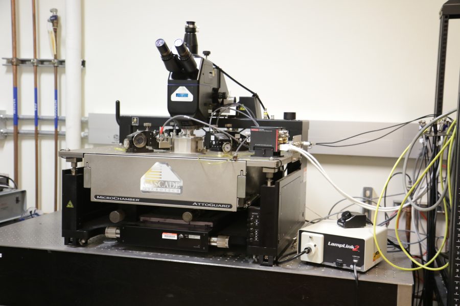
For electrical characterization and reliability measurements, the Electrical Characterization of Materials Evaluation Test Structures (eCOMETS) lab and Advanced Electrical Characterization laboratory (AECL) are jointly equipped with Cascade Summit series probe stations with integrated environmental control capable of probing structures on wafers (up to 200 mm diameter) over a temperature range of -65 to 200 °C is available. The probe station provides for current measurement down to fA and capacitance measurement down to tens of fF. A Lakeshore Cryogenic low temperature probe station is also available to expand the accessible temperature range and permit device level characterization on structures down to temperatures of ~4.5K.
Learn more on Dr. Chadwin Young’s research group page
Cleanroom Research Laboratory
The Cleanroom Research Laboratory is a facility that offers an excellent location for various technical organizations and companies to carryout research activities. The lab includes facilities for device fabrication and characterization with a range of equipment. It is a facility with filtered, vertical laminar flow air, equipped with versatile semiconductor process research equipment assembled for the purpose of supporting university research in the fields of microelectronics, electronic materials, nanotechnology, MEMS, lithography, optics, and other areas requiring a particle-free environment.
Nano-Characterization Facility
Focused Ion Beam/Scanning Electron Microscopy
For the nanoscale analysis of high-k/III-V stack structures, UTD is well equipped in state-of-the-art electron microscopy as well. A focused ion beam system available in the Advanced Microscopy Laboratory is a FEI Nova 200 NanoLab, which is a dual column SEM/FIB. It combines ultra-high resolution field emission scanning electron microscopy (SEM) and focused ion beam (FIB) etch and deposition for nanoscale prototyping, machining, 2-D and 3-D characterization, and analysis. Five gas injection systems are available for deposition (e.g. Pt, C, SiO2) and etching (e.g. Iodine for metals, and a dielectric etch). The FIB will be critical for TEM sample preparation of III-V compounds. Nanoscale chemical analysis is performed with energy dispersive X-ray spectroscopy (EDS). The secondary electron image resolution at the dual beam coincidence point is 1.5 nm at 15 kV. The FIB optics have better than 7 nm resolution at 30 kV. A high resolution digital patterning system controlled from the user interface is also available. Predefined device structures in Bitmap format can be directly imported to the patterning system for nanoscale fabrication. The FEI Nova 200 is also equipped with a Zyvex F100 nano-manipulation stage, which includes four manipulators with 10 nm positioning resolution. The four manipulators can be fitted with either sharp whisker probes for electrically probing samples or microgrippers for manipulating nanostructures as small as 10 nanometers. Students are trained to operate this instrument routinely by a dedicated full time staff member.
High-Resolution Transmission Electron Microcopy
The facility operates and maintains two state-of-the-art transmission electron microscopes (TEM), and a host of sample preparation equipment. It also provides microscopy computing and visualization capabilities. Techniques and equipment available includes the following: (i) High Resolution Structural Analysis – The high-resolution imaging TEM is a JEOL 2100 F which is a 200kV field emission TEM. Its capability includes atomic scale structural imaging with a resolution of better than 0.19 nm, and in-situ STM/TEM. (ii) High Resolution Chemical and Electronic Structure Analysis – High resolution analytical TEM is a second JEOL 2100F field emission TEM/STEM equipped with an energy dispersive x-ray spectrometer (EDS), an electron energy loss spectrometer (EELS), and a high angle Z-contrast imaging detector. This instrument performs chemical and electronic structure analysis with a spatial resolution of better than 0.5 nm in EELS mode and is also capable of spectrum imaging and mapping. The image resolution in the chemically sensitive Z-contrast scanning TEM (STEM) mode will be about 0.14 nm. Its capability also includes in-situ cryogenic cooling and heating, and a computer control system for remote microscopy operation.
X-ray Diffraction Suite
For the study of film microstructure and epitaxial quality, a new X-ray diffraction suite has been acquired by UTD to support nanotechnology thin film materials research. A Rigaku Ultima III X-ray Diffractometer system is available for thin film diffraction characterization. The system is equipped with a cross beam optics system to permit either high-resolution parallel beam with a motor controlled multilayer mirror, or a Bragg-Brentano para-focusing beam which are permanently mounted, pre-aligned and user selectable with no need for any interchange between components. Curved graphite crystal or Ge monochrometers are also available for high-resolution XRD measurements. An integrated annealing attachment permits the in-situ examination of film structure up to 1500°C.
The instrument enables a variety of applications including in-plane and normal geometry phase identification, quantitative analysis, lattice parameter refinement, crystallite size, structure refinement, residual stress, density, roughness (from reflectivity geometries), and depth-controlled phase identification. The advanced thin film attachments enable precise sample alignment for x-ray reflectivity, grazing-incidence x-ray diffraction, epitaxial film concentration and structure analysis using reciprocal space mapping and rocking curve measurements. Detection consists of a computer controlled scintillation counter. Sample sizes up to 100 mm in diameter can be accommodated on this system.
A Rigaku Rapid-Spider Image Plate Diffractometer system is also available for small spot (30μm – 300μm) XRD work. The digital image plate system enables the acquisition of diffraction data over a 2θ=204° angle with a rapid laser scanning readout system. An integrated annealing attachment permits the in-situ examination of film structure up to 900°C on this system.
A complete set of new control software, database, and analysis workstations is associated with these new systems. Students are trained to operate these instruments routinely by a dedicated full time staff member.
Learn more on Dr. Moon Kim’s research group page
Surface and Materials Characterization Laboratory
Surface and Materials Characterization Laboratory is available for students and researchers to investigate what elements (from the periodic table) compose the surface of a sample and how these elements are structured together. This is done by utilizing the VersaProbe II Scanning X-ray Photoelectron Spectroscopy microprobe, a multi-technique surface analysis instrument. Samples can be cleaned inside the system by an Argon cluster bombardment to remove the contaminants present at the surface. With the ion argon gun, it is also possible to atomically dig out the surface to investigate the inside of the sample.
- System: Physical Electronics Versa Probe II.
- Ultra-High Vacuum (UHV) base pressure: 4 10-8 Pa.
- Probing X-ray beam from 10×10 µm2 up to 200×200 µm2 made possible by Raster scanned, micro-focused, monochromatic x-ray beam.
- Large area mapping with micrometric resolution, XPS from small structures (15×15 µm2).
- Samples: conductors, semi-conductors, insulators (with charge compensation).
- Samples: solid, powder, organics, SAMS, etc… as long as they are UHV compatible.
- Sample size: 1×1 mm2 up to 2.5” Dia.
- Sputtering capabilities with Ar+ ion beam from 100 eV up to 5 KeV.
- Cleaning and mild sputtering with (Ar cluster)+ ion beam: cluster size from 1000 Ar atoms up to 2500 Ar atoms, beam energy from 2.5 KeV up to 25 KeV.
- UV capability: Our system is equipped with a He I/II UV lamp.
- Angle resolved UPS and XPS.
- Sample Temperature adjustable from -150oC up to 500oC.
CENTERS
Silicon Wafer Engineering and Defect Science (SiWEDS) Center
SiWEDS is a Graduated NSF Industry/University Cooperative Research Center. Research includes theory, experiment, modeling and simulation in four major interrelated tasks:
- Surface defects and contamination of wafers in device regions.
- Fundamentals and issues related to the elimination of bulk defects, and mechanisms and processes for gettering.
- Understanding wafers and alternate substrates such as Silicon on Insulator (SOI), Strained Silicon (sSi) on Bulk or Insulator (SSOI), GE on insulator (GEOI), etc.
- Developing metrology standards and new characterization techniques.