Faculty Research Summaries
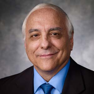
Orlando Auciello
Auciello is directing several basic and applied research programs on different fields, namely: 1) science and technology of multicomponent oxide thin films and application to devices (ferroelectric memories, novel correlated electron resistive change memories, nanoscale gates for complementary metal-oxide-semiconductor(CMOS) devices, photovoltaic energy-generation-storage devices, high-frequency devices, piezoelectric thin films micro-electromechanical systems/nanoelectromechanical systems (MEMS/NEMS) devices (sensors and actuators); 2) science and technology of a novel ultrananocrystalline diamond (UNCD) film, developed and patented by Auciello and his colleagues, and application to multifunctional devices and systems: a) UNCD coatings for electrodes, membranes and inner wall cases of Li-ion batteries (LIBs) with 10x longer life and safer than current LIBs; b) UNCD coating for implantable biomedical devices (artificial retina microchip, currently in the market, restoring partial sight to people blinded by retina photoreceptor degeneration), artificial heart valves, stents, artificial joints (hips, knees); c) UNCD scaffolds for developmental biology (cell growth and differentiation); biosensors; d) radio-frequency (RF) MEMS/NEMS; e) electron field emission cathodes (for flat-panel displays, mass spectrometers, X-ray sources); f) components with superior tribological performance (UNCD-coated mechanical pump seals, gears and other components, in the market by Advanced Diamond Technologies (company founded by Auciello and his colleagues in 2003); g) electrodes for fuel cells, catalysis, water purification and for neural stimulation.
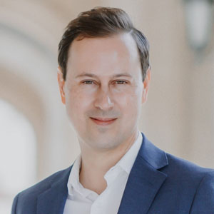
Kevin Brenner
Dr. Brenner’s research investigates the transport, conversion, and control of thermal and electrical energy. He is interested in both the fundamental limits of phonon and electron transport, and in materials or devices that can better control this energy. This research is applied to the engineering of electron devices, thermal packaging, and system reliability. His research group uses a range of experimental methods that provide connectivity from materials to devices and include Raman spectroscopy, nanoscale fabrication, and rigorous electrical and thermal transport measurements.
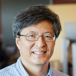
Kyeongjae (KJ) Cho
Dr. Kyeongjae Cho’s main area of research and teaching is multiscale modeling and simulation of nanoscale materials. In his research group (Multiscale Simulation Lab), diverse modeling tools are developed and applied to nanomaterial design. The modeling methods include atomistic and quantum simulations. Structure-property relationships of nanomaterials (nanoparticles, nanowires and nanoscale interfaces) are the main focus of modeling research. Research topics include metal nanoparticles, carbon nanotubes, semiconductor nanowires and high-k gate stack interface problems. Main applications areas are electronic device materials, biotechnology and clean energy technology.

Massimo (Max) V. Fischetti
Electronic transport in “large” semiconductor devices can be studied using simplifying assumptions afforded by the large size of the devices; mainly, the assumption of incoherent transport — amenable to the semi-classical Boltzmann picture — and of a “bulk-like” electronic structure of the conductive channel an assumption which permits the use of either the effective-mass approximation or of a “full-band” (but still bulk) description. Neither of these assumptions is valid in the “sub-5 nm era”. Novel materials (such as 2D materials and topological insulators), the small size of the devices, the strong quantum-confinement effects and the likelihood of quasi-coherent transport require major changes in how we study electronic transport. Our research proceeds on three fronts in order to tackle these problems: band-structure calculations (using Density-Functional Theory and Empirical Pseudopotentials), semi-classical electronic transport (using Monte Carlo simulations) and quantum transport (based on Empirical Pseudopotentials).
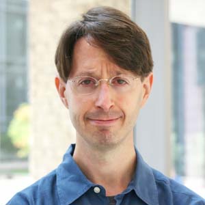
Lev Gelb
In molecular simulation research, powerful computers are used to accurately model real systems using statistical mechanics and quantum mechanics. This provides a sort of “virtual laboratory” in which almost any property can be measured or examined, including those which are not accessible to experiments. We use such simulations to develop an atomic scale understanding of the behavior of complex systems. Our current research is in two broad areas. The first is modeling the structure and properties of amorphous porous materials such as aerogels and colloidal gel networks, and the second is simulating chemical reaction thermodynamics in protic ionic liquids. Finally, we are involved in collaborative research on advanced methods for the analysis of experimental surface chemical imaging data.
Julia Hsu
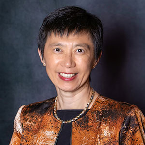
Dr. Julia Hsu’s research focuses on nanoscale materials physics; in particular nanomaterials for optoelectronic and energy applications. She has done extensive work on local characterization of electronic and photonic materials and devices using scanning probe techniques. The material systems she has studied include metals and alloys; group IV, III-V and II-VI semiconductors and oxides. She is most interested in how to tune macroscopic properties through materials synthesis and processing; e.g., band gap, work function or surface chemistry of inorganic nanoparticles. Specifically, her group focuses on the chemical and electronic properties at the organic-inorganic interface, with applications towards solar energy harvesting. Ongoing projects include organic photovoltaics, nanomaterial synthesis, solution processing of inorganic nanocrystals and thin films, synthesis and processing of few-layer transition metal dichalcogenides, electrical and optoelectronic studies of solar cells and transistors, nanocomposites for dielectric waveguides and earth-abundant oxides for toxic NOx abatement.

Jiyoung Kim
Research in Dr. Jiyoung Kim’s group focuses on innovative materials and their state-of-the-art devices employing atomic level process (atomic layer deposition [ALD], molecular layer deposition [MLD], atomic layer etching [ALE], etc.) for nanoelectronics, biomedical and energy devices applications. Advanced devices and applications include More Moore (scaling devices) and sub-5 nm complementary metal-oxide-semiconductor (CMOS) technology, advanced memory devices and memory-driven logics (ferroelectric memory, DRAMs/NANDs, memristors and memcapacitors), power/RF/analog device integration, multilevel interconnections and advanced packaging, flexible devices and sensor/energy devices. Innovative nanoscale materials include alternative channel materials (III-V, Ge, 2D-Graphene, TMD, MIT, etc.) organic-inorganic hybrid films, novel dielectrics (high-k, functional dielectrics, low-k dielectrics) and metals (metals that conduct oxide and nitride) and thermal spreader and barrier layers. Finally, Kim’s group studies atomically precise processes, including novel ALD/MLD/ALE systems, in situ characterization techniques, molecular layer deposition, selective ALD/ALE, epitaxial ALD, SiOx/SiNx ALD and ALD for 0D, 1D, 2D and 3D nano-structures.
Moon Kim
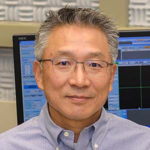
Dr. Moon Kim’s current research includes nanoscale fabrication and atomic scale characterization of various functional nanostructures/devices for applications in nanoelectronics, power electronics, energy, electrochemical and biodevices and virtual reality (VR) contents for enhanced education and Artificial Intelligence (AI) platforms for new emerging applications.
Kyle McCall
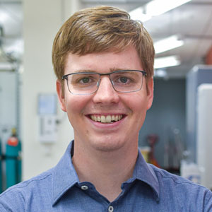
The McCall group encompasses the full range of materials chemistry, from the choice or design of prospective energy-related materials, to their successful incorporation into functioning devices such as solar cells or light emitting devices. This research focuses on the synthesis and characterization of complex semiconductors for energy applications, where the combined practice of materials science, chemistry, and physics enables structure-property relationships to be established and tested through the creation of novel materials. This work will bring the materials-by-design approach to bear on the energy-related problems of our time to enable next-generation sustainable materials. Semiconductor materials of interest include halide perovskites and other metal halides, as well as chalcohalides and chalcogenides. Current research topics include the following areas: Renewable Energy Conversion, Light Emission, and Radiation Detection.
Manuel Quevedo-Lopez
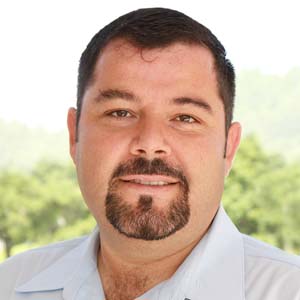
Flexible electronics is an exciting technology which requires expertise in several areas such as physics, chemistry and engineering. Therefore, the students in our group will not only gain experience with state-of-the-art instrumentation and techniques but also gain an understanding of the interdisciplinary nature of this area. Flexible electronics has many new applications, ranging from large area sensors to flexible displays to roll-up photovoltaics. However, to make flexible electronics a viable technology a number of key components still need to be developed including memory, logic, analog devices and amplifiers. Current projects include: sensors for detecting radiation, nano-engineered materials for flexible electronics, process integration (n-type metal-oxide-semiconductor or NMOS, pMOS, complementary metal-oxide-semiconductor or CMOS, etc.), device modeling and simulation, and energy harvesting and storage.

Laisuo su
Dr. Laisuo Su’s research focuses on developing revolutionary materials for renewable energy devices, especially in the area of rechargeable batteries such as lithium-ion batteries, sodium-ion batteries, and zinc-ion batteries. Among various components within a battery, the group has a particular interest in the electrolyte, including both liquid electrolyte and solid electrolyte, and electrolyte-electrode interface, where various critical reactions happen. The group is also interested in developing advanced characterization tools for monitoring chemical and electrochemical reactions happening in renewable energy devices to understand fundamental scientific research problems in the area of electrochemistry and materials science.
Cormac Toher
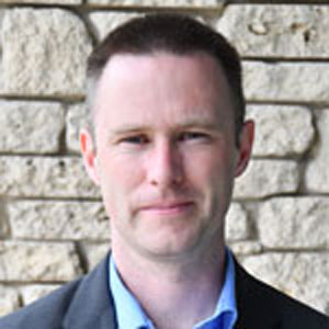
The Toher group’s research focuses on computational materials discovery and design, combining first-principles calculations, big data, machine-learning, and computational thermodynamics to predict the stability, synthesizability and properties of ordered and disordered materials. The group has a particular interest in high-entropy and amorphous materials such as high-entropy ceramics, which combine multiple elements on the cation sublattice to form an entropy-stabilized single-phase material with enhanced properties; and metallic glasses, which are metal alloys with an amorphous structure that can have enhanced mechanical properties and corrosion resistance. Current research interests include the development materials for extreme environments, such as high-entropy silicates to act as thermal and environmental barriers for hot section components of gas turbine engines. Other applications of interest range from components of nanoelectronic devices; to energy materials such as photovoltaics, thermoelectrics and catalysts.
William Vandenberghe
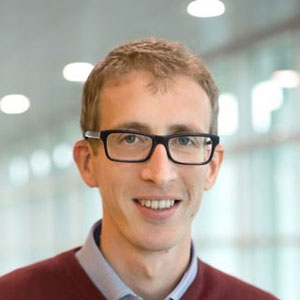
At the macroscopic scale, materials and devices can be described using classical and semiclassical physics, but at the nanoscale, quantum mechanical effects such as tunneling, quantum confinement or spin-orbit coupling are often dominant. While these quantum effects are mostly detrimental for performance in conventional devices such as transistors, quantum effects present a great opportunity for new devices. Our research focuses on the study of electron transport at the nanoscale using theoretical methods towards the development of new materials and devices. Specifically, we want to exploit quantum mechanical effects to realize new devices with improved performance, energy efficiency or new functionality. For example: 1) we analyze how band-to-band tunneling can be used to make transistors with very steep turn-on characteristics, 2) we determine the electronic conductivity and dielectric properties in new two-dimensional materials from first principles to seek out the most promising materials, 3) we study how the spin-polarized edge/surface states of topological insulators can lead to devices that are robust against defects and impurities or how fast and energy-efficient nano-scale magnetic memory devices can be fabricated or, 4) we study electron transport starting from first principles in noncrystalline nanoscale materials which is important for thin-film transistors or photovoltaics.

Walter Voit
The Advanced Polymer Research Lab uses shape memory polymers and other engineered plastics to solve problems in flexible electronics, neural interfaces, energy harvesting, acoustics, sensors and advanced manufacturing. Notable is the ability to insert penetrating neural implants while stiff and their ability to soften inside the body to lead to improved chronic responses. Research includes the thermomechanics of polymer systems and interface chemistry with thin-film conductors and organic semiconductors.
Amy Walker
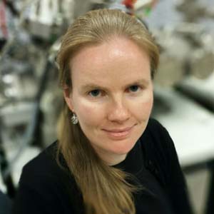
The ultimate goal of Dr. Amy Walker’s research is the development of simple, robust materials for constructing complex two- and three-dimensional surfaces by manipulating interfacial chemistry. Metal, semiconductor and biomolecular self-assembled monolayers or SAM structures have applications in organic electronics, sensing, catalysis, photovoltaics and optoelectronics. Her group also develops analytical techniques to probe the structures produced. The Walker group employs surface science techniques, in particular time-of-flight secondary-ion mass spectrometry (TOF SIMS) and reflection absorption infrared spectroscopy (RAIRS) and calculations of molecular structure (density functional theory, DFT) in this work. TOF SIMS is a unique widely applicable technique that provides detailed information about the chemical composition of surfaces with submicron lateral resolution and is used in areas ranging from biological systems to materials science.

Robert Wallace
Research in the Wallace group focuses on the study of surfaces and interfaces, particularly with applications to electronic materials and the resultant devices fabricated from them. Driven by integrated circuit scaling and industrial experience, our work has led to participation on several nationally renowned academic centers sponsored by the Semiconductor Research Corporation with tasks focusing on the interfacial physics and chemistry of metals and dielectrics in contact with semiconductor and semimetal surfaces and the resultant device behavior correlations. Our current interests include materials systems which (1) extend complementary metal-oxide-semiconductor (CMOS) devices as well as (2) materials systems leading to concepts beyond CMOS-based logic.

Chadwin Young
Research interests include electrical characterization and reliability methodologies. On novel characterization development we are involved in the measurement and evaluation of transistors and capacitors of experimental gate stacks and device structures (alternative gate electrodes, ultra-thin oxides, oxynitrides and high-dielectric constant insulators, nonplanar devices and high-mobility substrates). We are engaged in the electrical characterization and reliability of projected material and device architectures below the 22nm node as defined by the International Technology Roadmap for Semiconductors (ITRS) as well as other future device architectures, which can call for high-k dielectrics and high-mobility and/or flexible-substrate material systems.


